Arduino - emulating Shiftout (74HS595) - in mblock?


#1

Hi There, Im new to mblock, I’m using mblock5 with an arduino (with which I’m also newbie) to try to to teach my 7yo about all this stuff. Hence, I guess I want to avoid ‘C’ at this stage with him! So, we’ve done some basic projects, all good. We now are designing a scoreboard, for which I need to use a shift register (595) to shift data to a 7Segment4Digit display…

Has anyone had any experience in driving this chip using m’block. Ive tried to emulate the clock, latch and data timing in a basic loop but cant seem to clock or latch data in to this register from mblock…? (hence no luck displaying anything!). C code examples on my wired up project work ok, and drive the chip and display ok, so I know its just what Im trying to do in mblock…

Anyway, please be gentle with me. My credibility with a 7yo is on the line :wink: - and last time I wrote a program was in basic on an 8bit computer!

Thanks for any help, advice and suggestions!

Cheers


#2

Been a little while since using this chip but it is quite easy. Timing isn’t critical as the chip will go at what ever speed you pulse the clock pin at providing your not pulsing quicker than the chip can go.

Off memory it works like this set clock pin low then to starts transmission of bits pull latch pin low then to send each bit you first set the data to either high or low for what ever data you want to send then pulse the clock pin high then back to low to send it then repeat until all bits are sent then set latch pin high.


#3

Welcome Chris. Perhaps if you shared your working C code and your Mblock code we could offer some suggestions. Assuming the code is generally the same, the difference might be processing speed. Are you using live more or upload mode?


#4

Hi Folks,

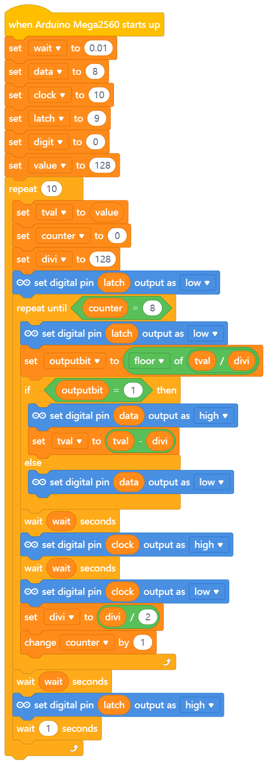
Thanks so much for looking at this. This is the mblock and the ‘c’ it generated, and following that is a paste of the sample program I have run successfully (which was compiled from the Arduino IDE. Apologies for the awful ‘code’ Im sure Im missing something really obvious - just cant see it!

Cheers
Chris

// generated by mBlock5 for
// codes make you happy

#include <Arduino.h>
#include <Wire.h>
#include <SoftwareSerial.h>

float counter = 0;
float latch = 0;
float clock = 0;
float data = 0;
float divi = 0;
float outputbit = 0;
float tval = 0;
float result = 0;
float wait = 0;
float digit = 0;
float value = 0;

void _delay(float seconds) {
long endTime = millis() + seconds * 1000;
while(millis() < endTime) _loop();
}

void setup() {
pinMode(latch,OUTPUT);
pinMode(data,OUTPUT);
pinMode(clock,OUTPUT);
wait = 0.01;
data = 8;
clock = 10;
latch = 9;
digit = 0;
value = 128;
for(int count=0;count<10;count++){
tval = value;
counter = 0;
divi = 128;
digitalWrite(latch,0);
while(!(counter == 8.000000))
{
_loop();
digitalWrite(latch,0);
outputbit = floor(tval / divi);
if(outputbit == 1.000000){
digitalWrite(data,1);
tval = ((tval - divi));

    }else{
        digitalWrite(data,0);

    }
    _delay(float(wait));
    digitalWrite(clock,1);
    _delay(float(wait));
    digitalWrite(clock,0);
    divi = divi / 2;
    counter += 1;

  }
  _delay(float(wait));
  digitalWrite(latch,1);
  _delay(1);

}

}

void _loop() {
}

void loop() {
_loop();
}

_sample program which works ok on the same board/prototype setup

//www.elegoo.com
//2016.12.12

// define the LED digit patterns, from 0 - 9
// 1 = LED on, 0 = LED off, in this order:
// 74HC595 pin Q0,Q1,Q2,Q3,Q4,Q5,Q6,Q7
// Mapping to a,b,c,d,e,f,g of Seven-Segment LED
byte seven_seg_digits[10] = { B11111100, // = 0
B01100000, // = 1
B11011010, // = 2
B11110010, // = 3
B01100110, // = 4
B10110110, // = 5
B10111110, // = 6
B11100000, // = 7
B11111110, // = 8
B11100110 // = 9
};

// connect to the ST_CP of 74HC595 (pin 3,latch pin)
int latchPin = 9;
// connect to the SH_CP of 74HC595 (pin 4, clock pin)
int clockPin = 10;
// connect to the DS of 74HC595 (pin 2)
int dataPin = 8;

void setup() {
// Set latchPin, clockPin, dataPin as output
pinMode(latchPin, OUTPUT);
pinMode(clockPin, OUTPUT);
pinMode(dataPin, OUTPUT);
}

// display a number on the digital segment display
void sevenSegWrite(byte digit) {
// set the latchPin to low potential, before sending data
digitalWrite(latchPin, LOW);

// the original data (bit pattern)
shiftOut(dataPin, clockPin, LSBFIRST, seven_seg_digits[digit]);

// set the latchPin to high potential, after sending data
digitalWrite(latchPin, HIGH);
}

void loop() {
// count from 9 to 0
for (byte digit = 10; digit > 0; --digit) {
delay(100);
sevenSegWrite(digit - 1);
}

// suspend 4 seconds
delay(100);
}


#5

PS, Im using upload mode (I wondered if live mode was part of the issue). Also these programs don’t do the same thing. My program is an attempt to light any segment on all digits (value), but the working test program does show the board, 595, and 7 seg 4 digit display does ‘light up’ correctly 1111 - 9999…so I dont think its hardware or my wiring!..


#6

OK first we have to fix your data types.

Your using float as a data type this won’t work.
I make a block to set a pin to on/off


#7

I will use this as it is cleaner than the if, then else… and does show me how to extend mblocks - so thankyou!.

Though, in my code I think im using a HIGH, LOW (1, 0) write to the data, clock and latch port, rather than the output bit - which is as you say a float/double - see the if, then else? Am I missing something obvious here?

I have checked the if then else on the output bit part - and all seems good, its detecting the 1’s and 0’s correctly in tval then writing HIGH or LOW directly to the pin…

Thanks for your help

Chris


#8

you need to put the setup code for the pins in the setup place

then place the function you call in the declare place
// display a number on the digital segment display
void sevenSegWrite(byte digit) {
// set the latchPin to low potential, before sending data
digitalWrite(latchPin, LOW);

// the original data (bit pattern)
shiftOut(dataPin, clockPin, LSBFIRST, seven_seg_digits[digit]);

// set the latchPin to high potential, after sending data
digitalWrite(latchPin, HIGH);
}

Then in the code place call that function and pass it the byte you want to send
"


#9

Hi, So are you describing creating your own block extension using raw C code?? I was trying to use low level mblock available commands such as set port HIGH, and set port LOW, and calculating the bit shifting so I (and my kids) can understand whats going on under the covers. I would like to see if I can figure out why the mblock code doesnt work, just so I can learn from mistakes.

Having said that I would like to try the extension method once I have more experience with mblock, just need to figure out if I can use the extension in my code or need to publish it?

Thanks again for taking the time to help, I really appreciate your ideas.

Chris


#10

ok if you want to go under the bonnet then I can explain how to do as this is what I usually do myself. I am more used to programming in C and Ardunio is new to me.

The function “shiftOut(dataPin, clockPin, LSBFIRST, seven_seg_digits[digit]);” is doing the work for you and I assume it is an Ardunio inbuilt function as I haven’t seen it before.

It will work like this. U want to send a byte to a shift register then you have to send 1 bit at a time until you have sent the 8 bits that make up a byte. This is done by you set the data pin to the value of that bit then pulse the clock pin (this tells the shift register to read the state of the data pin) then you set the data pin to the value of the next bit then pulse the clock line again.

So you need to learn how to pick off single bits from a byte. This can be done either starting at the MSB(most significant bit) or my starting at the LSB (least significant bit). You need to use a mask and the bit-wise operation “and” to pick off the bit. I will use 1 in the LSB position then and with the byte needs to be sent the shift the byte that needs to be sent then repeate

mask = 1;
digtialWrite(LatchPin, LOW) //let shift register know that I am starting transmission
for(int i=0; i<8; i++){
digitalWrite(dataPin, byte_to_be_sent & mask); //set data pin to LSB
byte_to_be_sent >>= 1 //shift byte to left 1 place
digitalWrite(clockPin, HIGH); //pulse clock pin
Delay (0.03);
digitalWrite(clockPin, LOW);
}
digtialWrite(LatchPin, HIGH) //let shift register know that I am finished transmission


#11

This is what my mblock code is trying to do (emulate) yes. However that doesnt work, and yes, shiftout is part of the ardiuino librariies from what I know and yes, to prove my hardware set up I used shiftout in one of the sample arduino C programs.

I would really appreciate any hints as to why the following code doesnt effectively mimic the shiftout snippet you provided above. Apologies I’m hanging onto this, as Id really like to teach my kids how to control the arduino using mblock - not C at this stage!

Cheers, and thanks for your patience


#12

Here’s the output of your mblock code. (I just copied the arduino code and inserted some debugging statements). Is this what you expect?

count 0 |tval 128.00 |
pin latch 9.00 low |pin latch 9.00 low |outputbit 1.00 |pin data 8.00 high |tval 0.00 |
pin clock 10.00 high |pin clock 10.00 low |divi 64.00 |pin latch 9.00 low |outputbit 0.00 |pin data 8.00 low |
pin clock 10.00 high |pin clock 10.00 low |divi 32.00 |pin latch 9.00 low |outputbit 0.00 |pin data 8.00 low |
pin clock 10.00 high |pin clock 10.00 low |divi 16.00 |pin latch 9.00 low |outputbit 0.00 |pin data 8.00 low |
pin clock 10.00 high |pin clock 10.00 low |divi 8.00 |pin latch 9.00 low |outputbit 0.00 |pin data 8.00 low |
pin clock 10.00 high |pin clock 10.00 low |divi 4.00 |pin latch 9.00 low |outputbit 0.00 |pin data 8.00 low |
pin clock 10.00 high |pin clock 10.00 low |divi 2.00 |pin latch 9.00 low |outputbit 0.00 |pin data 8.00 low |
pin clock 10.00 high |pin clock 10.00 low |divi 1.00 |pin latch 9.00 low |outputbit 0.00 |pin data 8.00 low |
pin clock 10.00 high |pin clock 10.00 low |divi 0.50 |pin latch 9.00 high |
count 1 |tval 128.00 |
pin latch 9.00 low |pin latch 9.00 low |outputbit 1.00 |pin data 8.00 high |tval 0.00 |
pin clock 10.00 high |pin clock 10.00 low |divi 64.00 |pin latch 9.00 low |outputbit 0.00 |pin data 8.00 low |
pin clock 10.00 high |pin clock 10.00 low |divi 32.00 |pin latch 9.00 low |outputbit 0.00 |pin data 8.00 low |
pin clock 10.00 high |pin clock 10.00 low |divi 16.00 |pin latch 9.00 low |outputbit 0.00 |pin data 8.00 low |
pin clock 10.00 high |pin clock 10.00 low |divi 8.00 |pin latch 9.00 low |outputbit 0.00 |pin data 8.00 low |
pin clock 10.00 high |pin clock 10.00 low |divi 4.00 |pin latch 9.00 low |outputbit 0.00 |pin data 8.00 low |
pin clock 10.00 high |pin clock 10.00 low |divi 2.00 |pin latch 9.00 low |outputbit 0.00 |pin data 8.00 low |
pin clock 10.00 high |pin clock 10.00 low |divi 1.00 |pin latch 9.00 low |outputbit 0.00 |pin data 8.00 low |
pin clock 10.00 high |pin clock 10.00 low |divi 0.50 |pin latch 9.00 high |
count 2 |tval 128.00 |
pin latch 9.00 low |pin latch 9.00 low |outputbit 1.00 |pin data 8.00 high |tval 0.00 |
pin clock 10.00 high |pin clock 10.00 low |divi 64.00 |pin latch 9.00 low |outputbit 0.00 |pin data 8.00 low |
pin clock 10.00 high |pin clock 10.00 low |divi 32.00 |pin latch 9.00 low |outputbit 0.00 |pin data 8.00 low |
pin clock 10.00 high |pin clock 10.00 low |divi 16.00 |pin latch 9.00 low |outputbit 0.00 |pin data 8.00 low |
pin clock 10.00 high |pin clock 10.00 low |divi 8.00 |pin latch 9.00 low |outputbit 0.00 |pin data 8.00 low |
pin clock 10.00 high |pin clock 10.00 low |divi 4.00 |pin latch 9.00 low |outputbit 0.00 |pin data 8.00 low |
pin clock 10.00 high |pin clock 10.00 low |divi 2.00 |pin latch 9.00 low |outputbit 0.00 |pin data 8.00 low |
pin clock 10.00 high |pin clock 10.00 low |divi 1.00 |pin latch 9.00 low |outputbit 0.00 |pin data 8.00 low |
pin clock 10.00 high |pin clock 10.00 low |divi 0.50 |pin latch 9.00 high |
count 3 |tval 128.00 |
pin latch 9.00 low |pin latch 9.00 low |outputbit 1.00 |pin data 8.00 high |tval 0.00 |
pin clock 10.00 high |pin clock 10.00 low |divi 64.00 |pin latch 9.00 low |outputbit 0.00 |pin data 8.00 low |
pin clock 10.00 high |pin clock 10.00 low |divi 32.00 |pin latch 9.00 low |outputbit 0.00 |pin data 8.00 low |
pin clock 10.00 high |pin clock 10.00 low |divi 16.00 |pin latch 9.00 low |outputbit 0.00 |pin data 8.00 low |
pin clock 10.00 high |pin clock 10.00 low |divi 8.00 |pin latch 9.00 low |outputbit 0.00 |pin data 8.00 low |
pin clock 10.00 high |pin clock 10.00 low |divi 4.00 |pin latch 9.00 low |outputbit 0.00 |pin data 8.00 low |
pin clock 10.00 high |pin clock 10.00 low |divi 2.00 |pin latch 9.00 low |outputbit 0.00 |pin data 8.00 low |
pin clock 10.00 high |pin clock 10.00 low |divi 1.00 |pin latch 9.00 low |outputbit 0.00 |pin data 8.00 low |
pin clock 10.00 high |pin clock 10.00 low |divi 0.50 |pin latch 9.00 high |
count 4 |tval 128.00 |
pin latch 9.00 low |pin latch 9.00 low |outputbit 1.00 |pin data 8.00 high |tval 0.00 |
pin clock 10.00 high |pin clock 10.00 low |divi 64.00 |pin latch 9.00 low |outputbit 0.00 |pin data 8.00 low |
pin clock 10.00 high |pin clock 10.00 low |divi 32.00 |pin latch 9.00 low |outputbit 0.00 |pin data 8.00 low |
pin clock 10.00 high |pin clock 10.00 low |divi 16.00 |pin latch 9.00 low |outputbit 0.00 |pin data 8.00 low |
pin clock 10.00 high |pin clock 10.00 low |divi 8.00 |pin latch 9.00 low |outputbit 0.00 |pin data 8.00 low |
pin clock 10.00 high |pin clock 10.00 low |divi 4.00 |pin latch 9.00 low |outputbit 0.00 |pin data 8.00 low |
pin clock 10.00 high |pin clock 10.00 low |divi 2.00 |pin latch 9.00 low |outputbit 0.00 |pin data 8.00 low |
pin clock 10.00 high |pin clock 10.00 low |divi 1.00 |pin latch 9.00 low |outputbit 0.00 |pin data 8.00 low |
pin clock 10.00 high |pin clock 10.00 low |divi 0.50 |pin latch 9.00 high |
count 5 |tval 128.00 |
pin latch 9.00 low |pin latch 9.00 low |outputbit 1.00 |pin data 8.00 high |tval 0.00 |
pin clock 10.00 high |pin clock 10.00 low |divi 64.00 |pin latch 9.00 low |outputbit 0.00 |pin data 8.00 low |
pin clock 10.00 high |pin clock 10.00 low |divi 32.00 |pin latch 9.00 low |outputbit 0.00 |pin data 8.00 low |
pin clock 10.00 high |pin clock 10.00 low |divi 16.00 |pin latch 9.00 low |outputbit 0.00 |pin data 8.00 low |
pin clock 10.00 high |pin clock 10.00 low |divi 8.00 |pin latch 9.00 low |outputbit 0.00 |pin data 8.00 low |
pin clock 10.00 high |pin clock 10.00 low |divi 4.00 |pin latch 9.00 low |outputbit 0.00 |pin data 8.00 low |
pin clock 10.00 high |pin clock 10.00 low |divi 2.00 |pin latch 9.00 low |outputbit 0.00 |pin data 8.00 low |
pin clock 10.00 high |pin clock 10.00 low |divi 1.00 |pin latch 9.00 low |outputbit 0.00 |pin data 8.00 low |
pin clock 10.00 high |pin clock 10.00 low |divi 0.50 |pin latch 9.00 high |
count 6 |tval 128.00 |
pin latch 9.00 low |pin latch 9.00 low |outputbit 1.00 |pin data 8.00 high |tval 0.00 |
pin clock 10.00 high |pin clock 10.00 low |divi 64.00 |pin latch 9.00 low |outputbit 0.00 |pin data 8.00 low |
pin clock 10.00 high |pin clock 10.00 low |divi 32.00 |pin latch 9.00 low |outputbit 0.00 |pin data 8.00 low |
pin clock 10.00 high |pin clock 10.00 low |divi 16.00 |pin latch 9.00 low |outputbit 0.00 |pin data 8.00 low |
pin clock 10.00 high |pin clock 10.00 low |divi 8.00 |pin latch 9.00 low |outputbit 0.00 |pin data 8.00 low |
pin clock 10.00 high |pin clock 10.00 low |divi 4.00 |pin latch 9.00 low |outputbit 0.00 |pin data 8.00 low |
pin clock 10.00 high |pin clock 10.00 low |divi 2.00 |pin latch 9.00 low |outputbit 0.00 |pin data 8.00 low |
pin clock 10.00 high |pin clock 10.00 low |divi 1.00 |pin latch 9.00 low |outputbit 0.00 |pin data 8.00 low |
pin clock 10.00 high |pin clock 10.00 low |divi 0.50 |pin latch 9.00 high |
count 7 |tval 128.00 |
pin latch 9.00 low |pin latch 9.00 low |outputbit 1.00 |pin data 8.00 high |tval 0.00 |
pin clock 10.00 high |pin clock 10.00 low |divi 64.00 |pin latch 9.00 low |outputbit 0.00 |pin data 8.00 low |
pin clock 10.00 high |pin clock 10.00 low |divi 32.00 |pin latch 9.00 low |outputbit 0.00 |pin data 8.00 low |
pin clock 10.00 high |pin clock 10.00 low |divi 16.00 |pin latch 9.00 low |outputbit 0.00 |pin data 8.00 low |
pin clock 10.00 high |pin clock 10.00 low |divi 8.00 |pin latch 9.00 low |outputbit 0.00 |pin data 8.00 low |
pin clock 10.00 high |pin clock 10.00 low |divi 4.00 |pin latch 9.00 low |outputbit 0.00 |pin data 8.00 low |
pin clock 10.00 high |pin clock 10.00 low |divi 2.00 |pin latch 9.00 low |outputbit 0.00 |pin data 8.00 low |
pin clock 10.00 high |pin clock 10.00 low |divi 1.00 |pin latch 9.00 low |outputbit 0.00 |pin data 8.00 low |
pin clock 10.00 high |pin clock 10.00 low |divi 0.50 |pin latch 9.00 high |
count 8 |tval 128.00 |
pin latch 9.00 low |pin latch 9.00 low |outputbit 1.00 |pin data 8.00 high |tval 0.00 |
pin clock 10.00 high |pin clock 10.00 low |divi 64.00 |pin latch 9.00 low |outputbit 0.00 |pin data 8.00 low |
pin clock 10.00 high |pin clock 10.00 low |divi 32.00 |pin latch 9.00 low |outputbit 0.00 |pin data 8.00 low |
pin clock 10.00 high |pin clock 10.00 low |divi 16.00 |pin latch 9.00 low |outputbit 0.00 |pin data 8.00 low |
pin clock 10.00 high |pin clock 10.00 low |divi 8.00 |pin latch 9.00 low |outputbit 0.00 |pin data 8.00 low |
pin clock 10.00 high |pin clock 10.00 low |divi 4.00 |pin latch 9.00 low |outputbit 0.00 |pin data 8.00 low |
pin clock 10.00 high |pin clock 10.00 low |divi 2.00 |pin latch 9.00 low |outputbit 0.00 |pin data 8.00 low |
pin clock 10.00 high |pin clock 10.00 low |divi 1.00 |pin latch 9.00 low |outputbit 0.00 |pin data 8.00 low |
pin clock 10.00 high |pin clock 10.00 low |divi 0.50 |pin latch 9.00 high |
count 9 |tval 128.00 |
pin latch 9.00 low |pin latch 9.00 low |outputbit 1.00 |pin data 8.00 high |tval 0.00 |
pin clock 10.00 high |pin clock 10.00 low |divi 64.00 |pin latch 9.00 low |outputbit 0.00 |pin data 8.00 low |
pin clock 10.00 high |pin clock 10.00 low |divi 32.00 |pin latch 9.00 low |outputbit 0.00 |pin data 8.00 low |
pin clock 10.00 high |pin clock 10.00 low |divi 16.00 |pin latch 9.00 low |outputbit 0.00 |pin data 8.00 low |
pin clock 10.00 high |pin clock 10.00 low |divi 8.00 |pin latch 9.00 low |outputbit 0.00 |pin data 8.00 low |
pin clock 10.00 high |pin clock 10.00 low |divi 4.00 |pin latch 9.00 low |outputbit 0.00 |pin data 8.00 low |
pin clock 10.00 high |pin clock 10.00 low |divi 2.00 |pin latch 9.00 low |outputbit 0.00 |pin data 8.00 low |
pin clock 10.00 high |pin clock 10.00 low |divi 1.00 |pin latch 9.00 low |outputbit 0.00 |pin data 8.00 low |
pin clock 10.00 high |pin clock 10.00 low |divi 0.50 |pin latch 9.00 high |


#13

You will need to wrap up the digitalWrite function so it can be called from scratch I show here the 1 that I made https://www.youtube.com/watch?v=IMF2uohqpdM&feature=youtu.be

You will also need to wrap up the binary shift left operator


#14

Thankyou, thats going to be really helpful. Im sure with this headstart I’ll get the hang of this!


#15

This is very interesting. I can see with a value of 128 I’d be expecting 1 0 0 0 0 0 0 0 in the count loop to shift…im getting only 7 output bits - so this gives me some hope. Thankyou, I’ll let you know how I go with this. PS. Would you mind sharing how you add your debug lines - I presume its either using the mblock console, or a serial monitor?

Cheers, and thanks again for the help!


#16

Hi, I simply copied the code from MBLOCK into the Arduino sketch application and ran the code from there using the serial monitor as you suggest - a fairly tedious operation because every time you modified MBLOCK code you’d have to repeat this exercise, but it’s the only way I could think of to visualise the outputs.

Snippets of code below

      for(int count=0;count<10;count++){
          Serial.print("count "); Serial.print(count); Serial.print(" |");
          tval = value;
          Serial.print("tval "); Serial.print(tval); Serial.println(" |");
          counter = 0;
          divi = 128;

          digitalWrite(latch,0);
          Serial.print("pin latch "); Serial.print(latch); Serial.print(" low |");  
          while(!(counter == 8.000000))
          {

etc!


#17

Hi, Thanks…hadn’t thought of that. I’d assume there might be a way to write to the serial monitor/console in mblock, in upload mode? Maybe Im getting ahead of myself! Again thankyou for shedding some light on what might be going on! Will update if I get anywhere with it…


#18

I have ordered a a HC-05 Bluetooth module that simulates a com port from your PC to the UART post on your Ardunio over Bluetooth. Once it arrives then I plan to connect to 2 one of the other UART posts on the Auriga board (meag2560) and open a serial terminal on my computer to receive debug info.


#19

Now that is the biz!. Many $ for that BT module?


#20

suspect you may not have had a debug line in the then as well as else on the if ! im getting 8 bits…however, convinced that outofthebots iss right its to do with data types, though i am writing 1 and 0 to the ports NOT variables. ?? still havent figured it out - will keep looking!